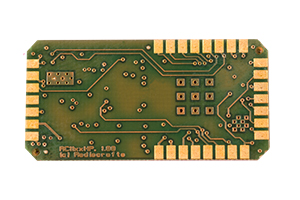
When designing the PCB layout for the RF modules, there are some measures that need to be taken to get the best performance from the radio module.
In our latest application note, AN061: RF PCB Layout Recommendations, we suggest some best practices for your product to succeed.
In addition, the Radiocrafts support team is always available to do a board layout review if you need someone to look over your design before production.
 In this application note you will learn about:
- The PCB materials used
- PCB stack-up and ground planes
- PCB transmission line types
- The interface between the module and the transmission line
- Module grounding
- Corners and vias
- Coax interface
You will also find examples of PCB layout in some of our reference designs posted on our website.
Download the application note here!

